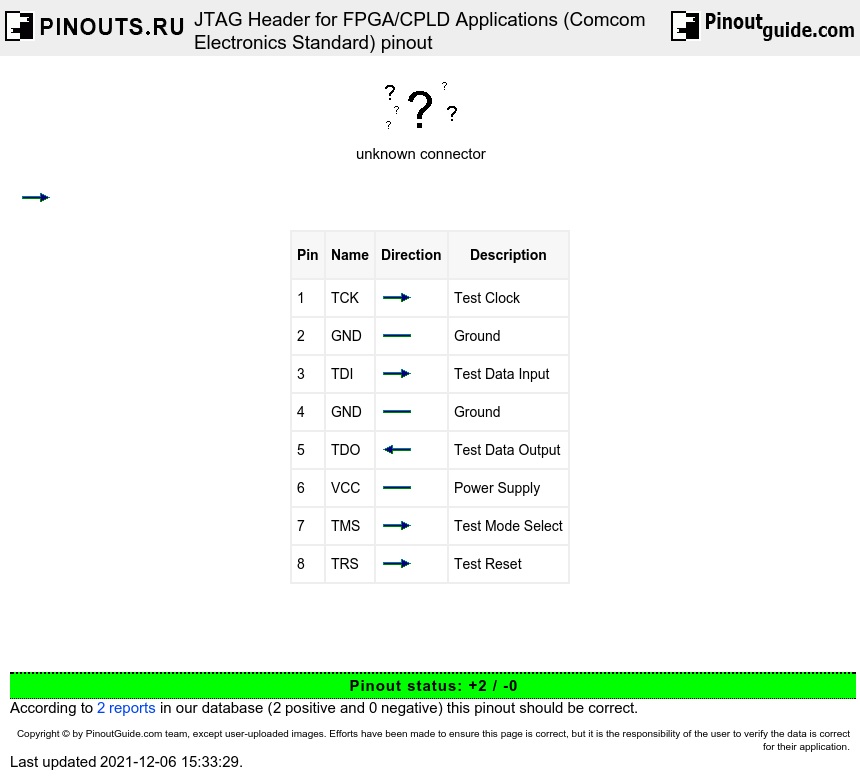
Hardware pinouts information and cables schemes

JTAG Header for FPGA/CPLD Applications (Comcom Electronics Standard) pinout

connector wiring scheme

bookmark this page

Pin Name Direction Description
1TCKTest Clock
2GNDGround
3TDITest Data Input
4GNDGround
5TDOTest Data Output
6VCCPower Supply
7TMSTest Mode Select
8TRSTest Reset

This information should be correct, but may be not. Please, help us to improve this document!
Is this document CORRECT or INCORRECT? Your opinion will be used to establish document status (showed at the bottom).

Want to add or correct something here? Edit this page!
Pinouts.ru > Some peripheral devices pinouts > Pinout of JTAG Header for FPGA/CPLD Applications (Comcom Electronics Standard) and layout of connector
Is it correct?:
should be correct
Source(s) of this and additional information: www.comcom.ru and Sandy
2 reports
Last updated 2008-06-28 21:56:54. Edit this page. Is this document correct or incorrect? What is your opinion?
[Discuss at the forum] [Back to index] [SUBMIT new pinout]
This page contain parts under Copyright © 2000-2008 by pinouts.ru team.
No any portion of this webpage may be reproduced in any form without visible direct link to this page provided. Webmaster permission required in any other cases.
Efforts have been made to ensure this page is correct, but it is the responsibility of the user to verify the data is correct for their application.
20409 hits since March 4, 2005