
CardBus, the 32-bit high performance bus mastering architecture for PC Cards, was standardized by the PCMCIA in May 1996. This bus is targeted to mobile computers. PCI-like 32-bit interface operates at a power-saving 3.3 volts, and cards can include standardized power-management mechanisms. The CardBus interface allows an I/O adapter or a memory module to be added to or removed without disrupting the systems operation. It adds high bandwidth PCI-based capabilities to the PC Card technology.
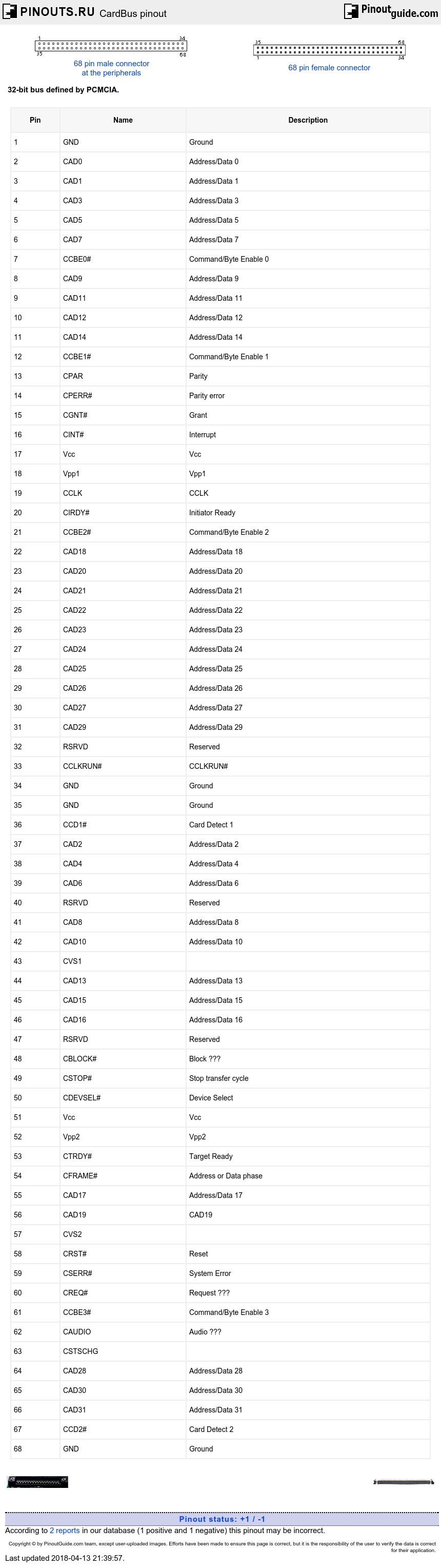
CardBus PC Cards are attached to their host system through a sturdy 68-pin connector, which is common to all PC Cards. (CardBus cards employ a shielding shroud around this connector, to enhance their signal integrity).
CardBus cards adopt the well-established PC Card form-factors. There are different types of CardBus cards (sizes are TxLxW):
- Type I: 3.3mm x 85.6mm x 54.0mm
- Type II: 5.0mm x 85.6mm x 54.0mm
- Type III: 10.5mm x 85.6mm x 54.0mm
CardBus provides a 32-bit multiplexed address/data path, which operates at PCI local-bus speeds of up to 33 MHz, yielding a peak bandwidth of 132MB/sec. CardBus accomplishes this by adopting the synchronous burst-transfer orientation of PCI, as well as a bus protocol, which is essentially identical to that of PCI.
| Pin | Name | Description |
|---|---|---|
| 1 | GND | Ground |
| 2 | CAD0 | Address/Data 0 |
| 3 | CAD1 | Address/Data 1 |
| 4 | CAD3 | Address/Data 3 |
| 5 | CAD5 | Address/Data 5 |
| 6 | CAD7 | Address/Data 7 |
| 7 | CCBE0# | Command/Byte Enable 0 |
| 8 | CAD9 | Address/Data 9 |
| 9 | CAD11 | Address/Data 11 |
| 10 | CAD12 | Address/Data 12 |
| 11 | CAD14 | Address/Data 14 |
| 12 | CCBE1# | Command/Byte Enable 1 |
| 13 | CPAR | Parity |
| 14 | CPERR# | Parity error |
| 15 | CGNT# | Grant |
| 16 | CINT# | Interrupt |
| 17 | Vcc | Vcc |
| 18 | Vpp1 | Vpp1 |
| 19 | CCLK | CCLK |
| 20 | CIRDY# | Initiator Ready |
| 21 | CCBE2# | Command/Byte Enable 2 |
| 22 | CAD18 | Address/Data 18 |
| 23 | CAD20 | Address/Data 20 |
| 24 | CAD21 | Address/Data 21 |
| 25 | CAD22 | Address/Data 22 |
| 26 | CAD23 | Address/Data 23 |
| 27 | CAD24 | Address/Data 24 |
| 28 | CAD25 | Address/Data 25 |
| 29 | CAD26 | Address/Data 26 |
| 30 | CAD27 | Address/Data 27 |
| 31 | CAD29 | Address/Data 29 |
| 32 | RSRVD | Reserved |
| 33 | CCLKRUN# | CCLKRUN# |
| 34 | GND | Ground |
| 35 | GND | Ground |
| 36 | CCD1# | Card Detect 1 |
| 37 | CAD2 | Address/Data 2 |
| 38 | CAD4 | Address/Data 4 |
| 39 | CAD6 | Address/Data 6 |
| 40 | RSRVD | Reserved |
| 41 | CAD8 | Address/Data 8 |
| 42 | CAD10 | Address/Data 10 |
| 43 | CVS1 | |
| 44 | CAD13 | Address/Data 13 |
| 45 | CAD15 | Address/Data 15 |
| 46 | CAD16 | Address/Data 16 |
| 47 | RSRVD | Reserved |
| 48 | CBLOCK# | Block ??? |
| 49 | CSTOP# | Stop transfer cycle |
| 50 | CDEVSEL# | Device Select |
| 51 | Vcc | Vcc |
| 52 | Vpp2 | Vpp2 |
| 53 | CTRDY# | Target Ready |
| 54 | CFRAME# | Address or Data phase |
| 55 | CAD17 | Address/Data 17 |
| 56 | CAD19 | CAD19 |
| 57 | CVS2 | |
| 58 | CRST# | Reset |
| 59 | CSERR# | System Error |
| 60 | CREQ# | Request ??? |
| 61 | CCBE3# | Command/Byte Enable 3 |
| 62 | CAUDIO | Audio ??? |
| 63 | CSTSCHG | |
| 64 | CAD28 | Address/Data 28 |
| 65 | CAD30 | Address/Data 30 |
| 66 | CAD31 | Address/Data 31 |
| 67 | CCD2# | Card Detect 2 |
| 68 | GND | Ground |
Another representation (looking into card)
| GND | 1 | 35 | GND | ||
| CAD0 | <-> | 2 | 36 | --> | !CCD1 |
| CAD1 | <-> | 3 | 37 | <-> | CAD2 |
| CAD3 | <-> | 4 | 38 | <-> | CAD4 |
| CAD5 | <-> | 5 | 39 | <-> | CAD6 |
| CAD7 | <-> | 6 | 40 | - | RSRVD |
| !CCBE0 | --> | 7 | 41 | <-> | CAD8 |
| CAD9 | <-> | 8 | 42 | <-> | CAD10 |
| CAD11 | <-> | 9 | 43 | - | CVS1 |
| CAD12 | <-> | 10 | 44 | <-> | CAD13 |
| CAD14 | <-> | 11 | 45 | <-> | CAD15 |
| !CCBE1 | --> | 12 | 46 | <-> | CAD16 |
| CPAR | --> | 13 | 47 | --- | RSRVD |
| !CPERR | --> | 14 | 48 | - | !CBLOCK |
| !CGNT | --> | 15 | 49 | - | !CSTOP |
| !CINT | --> | 16 | 50 | - | !CDEVSEL |
| Vcc | --> | 17 | 51 | <-- | Vcc |
| Vpp1 | --> | 18 | 52 | <-- | Vpp2 |
| CCLK | --> | 19 | 53 | - | !CTRDY |
| !CIRDY | - | 20 | 54 | - | !CFRAME |
| !CCBE2 | --> | 21 | 55 | <-> | CAD17 |
| CAD18 | <-> | 22 | 56 | <-> | CAD19 |
| CAD20 | <-> | 23 | 57 | - | CVS2 |
| CAD21 | <-> | 24 | 58 | <-- | !CRST |
| CAD22 | <-> | 25 | 59 | - | !CSERR |
| CAD23 | <-> | 26 | 60 | - | !CREQ |
| CAD24 | <-> | 27 | 61 | <-- | !CCBE3 |
| CAD25 | <-> | 28 | 62 | --> | CAUDIO |
| CAD26 | <-> | 29 | 63 | - | CSTSCHG |
| CAD27 | <-> | 30 | 64 | <-> | CAD28 |
| CAD29 | <-> | 31 | 65 | <-> | CAD30 |
| RSRVD | --- | 32 | 66 | <-> | CAD31 |
| !CCLKRUN | <-- | 33 | 67 | --> | !CCD2 |
| GND | --- | 34 | 68 | --- | GND |

 correct
 incorrect