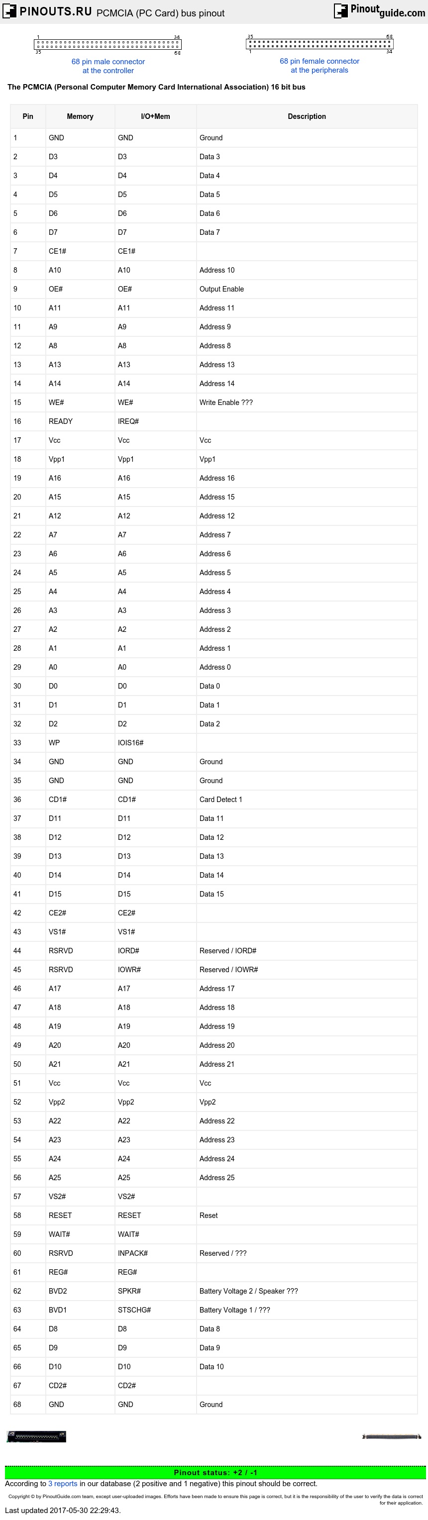
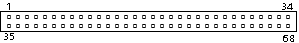

16-bit bus defined by PCMCIA.
PCMCIA Cards have 68 pin assignments, and interface with both 8- and 16-bit buses. They also support physical access of up to 64 MB of memory. PCMCIA cards give you universal expansion capability for mobile computers, and can support a variety of functions including wireline and radio-based fax and modem capabilities, mass storage, and memory extension for host machines.
There are three types of PCMCIA slots, identified by the thickness of the card that fits in them. All types are backward compatible.
Type I Cards are 3.3 mm thick. They"re used primarily in Personal Digital Assistants (PDAS) and handheld devices as RAM, FLASH memory, electrically erasable programmable read-only memory (EEPROM), and one-time programmable memory (OTP).
Type II Cards are 5 mm thick and are fully 1/0-capable. You can use them for memory enhancements or for 1/0 features in modems, LAN connections, and host communications.
Type III Cards measure 10.5 mm thick. They"re designed primarily for removable hard drives and radio communication devices which require a larger size. They can also be used for memory enhancements.
Miniature Cards are 3.5mm thick
The implementation of PCMCIA (PC Card) is based on the 8/16 bit data ISA bus (24-bit address bus)
| Pin | Memory | I/O+Mem | Description |
|---|---|---|---|
| 1 | GND | GND | Ground |
| 2 | D3 | D3 | Data 3 |
| 3 | D4 | D4 | Data 4 |
| 4 | D5 | D5 | Data 5 |
| 5 | D6 | D6 | Data 6 |
| 6 | D7 | D7 | Data 7 |
| 7 | CE1# | CE1# | |
| 8 | A10 | A10 | Address 10 |
| 9 | OE# | OE# | Output Enable |
| 10 | A11 | A11 | Address 11 |
| 11 | A9 | A9 | Address 9 |
| 12 | A8 | A8 | Address 8 |
| 13 | A13 | A13 | Address 13 |
| 14 | A14 | A14 | Address 14 |
| 15 | WE# | WE# | Write Enable ??? |
| 16 | READY | IREQ# | |
| 17 | Vcc | Vcc | Vcc |
| 18 | Vpp1 | Vpp1 | Vpp1 |
| 19 | A16 | A16 | Address 16 |
| 20 | A15 | A15 | Address 15 |
| 21 | A12 | A12 | Address 12 |
| 22 | A7 | A7 | Address 7 |
| 23 | A6 | A6 | Address 6 |
| 24 | A5 | A5 | Address 5 |
| 25 | A4 | A4 | Address 4 |
| 26 | A3 | A3 | Address 3 |
| 27 | A2 | A2 | Address 2 |
| 28 | A1 | A1 | Address 1 |
| 29 | A0 | A0 | Address 0 |
| 30 | D0 | D0 | Data 0 |
| 31 | D1 | D1 | Data 1 |
| 32 | D2 | D2 | Data 2 |
| 33 | WP | IOIS16# | |
| 34 | GND | GND | Ground |
| 35 | GND | GND | Ground |
| 36 | CD1# | CD1# | Card Detect 1 |
| 37 | D11 | D11 | Data 11 |
| 38 | D12 | D12 | Data 12 |
| 39 | D13 | D13 | Data 13 |
| 40 | D14 | D14 | Data 14 |
| 41 | D15 | D15 | Data 15 |
| 42 | CE2# | CE2# | |
| 43 | VS1# | VS1# | |
| 44 | RSRVD | IORD# | Reserved / IORD# |
| 45 | RSRVD | IOWR# | Reserved / IOWR# |
| 46 | A17 | A17 | Address 17 |
| 47 | A18 | A18 | Address 18 |
| 48 | A19 | A19 | Address 19 |
| 49 | A20 | A20 | Address 20 |
| 50 | A21 | A21 | Address 21 |
| 51 | Vcc | Vcc | Vcc |
| 52 | Vpp2 | Vpp2 | Vpp2 |
| 53 | A22 | A22 | Address 22 |
| 54 | A23 | A23 | Address 23 |
| 55 | A24 | A24 | Address 24 |
| 56 | A25 | A25 | Address 25 |
| 57 | VS2# | VS2# | |
| 58 | RESET | RESET | Reset |
| 59 | WAIT# | WAIT# | |
| 60 | RSRVD | INPACK# | Reserved / ??? |
| 61 | REG# | REG# | |
| 62 | BVD2 | SPKR# | Battery Voltage 2 / Speaker ??? |
| 63 | BVD1 | STSCHG# | Battery Voltage 1 / ??? |
| 64 | D8 | D8 | Data 8 |
| 65 | D9 | D9 | Data 9 |
| 66 | D10 | D10 | Data 10 |
| 67 | CD2# | CD2# | |
| 68 | GND | GND | Ground |
Another representation (look into card):
| Mem | I/O+Mem | Mem | I/O+Mem | ||||
| GND | --- | 1 | 35 | --- | GND | ||
| D3 | <-> | 2 | 36 | --> | !CD1 | ||
| D4 | <-> | 3 | 37 | <-> | D11 | ||
| D5 | <-> | 4 | 38 | <-> | D12 | ||
| D6 | <-> | 5 | 39 | <-> | D13 | ||
| D7 | <-> | 6 | 40 | <-> | D14 | ||
| !CE1 | - | 7 | 41 | <-> | D15 | ||
| A10 | --> | 8 | 42 | <-- | !CE2 | ||
| !OE | --> | 9 | 43 | - | !VS1 | ||
| A11 | --> | 10 | 44 | <-- | RSRVD | !IORD | |
| A9 | --> | 11 | 45 | <-- | RSRVD | !IOWR | |
| A8 | --> | 12 | 46 | <-- | A17 | ||
| A13 | --> | 13 | 47 | <-- | A18 | ||
| A14 | --> | 14 | 48 | <-- | A19 | ||
| !WE | --> | 15 | 49 | <-- | A20 | ||
| READY | !IREQ | --> | 16 | 50 | <-- | A21 | |
| Vcc | --> | 17 | 51 | <-- | Vcc | ||
| Vpp1 | --> | 18 | 52 | <-- | Vpp2 | ||
| A16 | --> | 19 | 53 | <-- | A22 | ||
| A15 | --> | 20 | 54 | <-- | A23 | ||
| A12 | --> | 21 | 55 | <-- | A24 | ||
| A7 | --> | 22 | 56 | <-- | A25 | ||
| A6 | --> | 23 | 57 | - | !VS2 | ||
| A5 | --> | 24 | 58 | <-- | RESET | ||
| A4 | --> | 25 | 59 | --> | !WAIT | ||
| A3 | --> | 26 | 60 | - | RSRVD | !INPACK | |
| A2 | --> | 27 | 61 | - | !REG | ||
| A1 | --> | 28 | 62 | --> | BVD2 | !SPKR | |
| A0 | --> | 29 | 63 | - | BVD1 | !STSCHG | |
| D0 | <-> | 30 | 64 | <-> | D8 | ||
| D1 | <-> | 31 | 65 | <-> | D9 | ||
| D2 | <-> | 32 | 66 | <-> | D10 | ||
| WP | !IOIS16 | --> | 33 | 67 | --> | !CD2 | |
| GND | --- | 34 | 68 | --- | GND | ||

 correct
 incorrect