

PSX controllers are intelligent devices and communicate with the Playstation device using a special syncrosound serial bus and protocol. The controller system is implemented in bus architechture, which means that all signal wires are all tied together in PSX end (except select which is seperate for each device).
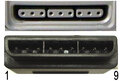
| Pin | Name | Description |
|---|---|---|
| 1 | DATA | Data |
| 2 | CMD | Command |
| 3 | +7.6V |
Dualshock and Dualshock 2 uses this for powering vibro-motors. Voltage on PS2 is 7.6V, however many sites says it's 9V. But it will work on 9V too. |
| 4 | GND | Ground |
| 5 | VCC | Vcc |
| 6 | ATT | ATT select |
| 7 | CLK | Clock ~7kHz |
| 8 | N/C | Not connected |
| 9 | ACK | Acknowledge |
PSX Signals descriptions:
Note: The ps1 digital joystick is Rising edge triggering, not falling edge.
DATA Signal from Controller to PSX.
This signal is an 8 bit serial transmission synchronous to the falling edge of clock (That is both the incoming and outgoing signals change on a high to low transition of clock. All the reading of signals is done on the leading edge to allow settling time.)
COMMAND Signal from PSX to Controller.
This signal is the counter part of DATA. It is again an 8 bit serial transmission on the falling edge of clock.
VCC VCC can vary from 5V down to 3V. The official SONY Controllers will operate on 3.3V, and not on 5V, however the unofficial controllers mostly will work on 5V. All controlers WILL work on 3.3V.
The main board in the PSX also has a surface mount 750mA fuse that will blow if you try to draw to much current through the plug (750mA is for both left, right and memory cards).
ATT ATT is used to get the attention of the controller.
This signal will go low for the duration of a transmission. I have also seen this pin called Select, DTR and Command.
CLOCK Signal from PSX to Controller.
Used to keep units in sync.
ACK Acknowledge signal from Controller to PSX.
This signal should go low for at least one clock period after each 8 bits are sent and ATT is still held low. If the ACK signal does not go low within about 60 us the PSX will then start interogating other devices.
It should also be noted that this is a bus of sorts. This means that the wires are all tied together (except select which is seperate for each device). For the CLK, ATT, and CMD pins this does not matter as the PSX is always the originator. The DATA and ACK pins however can be driven from any one of four devices. To avoid contentions on these lines they are open collectors and can only be driven low.
How to connect Playstation joystick to PC ?
It is possible to adapt a joystick originally developed for PSX to a PC. After connecting joystick to PC parallel port, you must install a driver so the operating system understands that the device connected is a joystick.
DB25                PSX
25 pin D-sub        9 pin
male                male
2--------------------------2
3--------------------------6
4--------------------------7
5--->|---|
6--->|---|
7--->|---|-----------------5
8--->|---|
9--->|---|
10-------------------------1
12-------------------------9
18,19----------------------4
->| means 1N4148 diode
18,19 shorted in cable
Also, you may connect pin 3 of PSX male to +5V to +9V
on external power supply to get vibration, and GND to pin 4.
The diodes better to be soldered inside the DB25 connector. Joystick with this cable will work only after manual drivers install. DirectPad drivers for Windows 2000 or XP may be downloaded from http://www.emulatronia.com/reportajes/directpad/ntpad.zip.
The PSX Controller Signals
All transmissions are eight bit serial LSB first. All timing in the PSX controller bus is syncronous to the falling edge of the clock. One byte of the transmissions will look kinda like this.
               |BIT 0|BIT 1|BIT 2|BIT 3|BIT 4|BIT 5|BIT 6|BIT 7|

    CLOCK -----___---___---___---___---___---___---___---___-----------

    DATA  -----000000111111222222333333444444555555666666777777--------

                  *     *     *     *     *     *     *     *

    CMND  -----000000111111222222333333444444555555666666777777--------

    ACK   ----------------------------------------------------------__-
The logic level on the data lines is changed by the transmitting device on the falling edge of clock. This is then read by the receiving device on the leading edge (at the points marked *) allowing time for the signal to settle. After each COMMAND is recieved by a selected controller, that controller needs to pull ACK low for at least one clock tick. If a selected controller does not ACK the PSX will assume that there is no controller present.
When the PSX wants to read information from a controller it pulls that devices ATT line low and issues a start command (0x01). The Controller Will then reply with its ID (0x41=Digital, 0x23=NegCon, 0x73=Analogue Red LED, 0x53=Analogue Green LED). At the same time as the controller is sending this ID byte the PSX is transmitting 0x42 to request the data. Following this the COMMAND line goes idle and the controller transmits 0x5A to say here comes the data.
This would look like this for a digital controller
    ATT    -______________________________________________________________

              |   Byte 1     |    |   Byte 2     |    |   Byte 3     |

    CLOCK  ---_-_-_-_-_-_-_-_-----_-_-_-_-_-_-_-_-----_-_-_-_-_-_-_-_-----

                   0xFF                0x41                0x5A

    DATA   -------------------------__________--__----__--__----__--__----

                   0x01                0x42

    CMND   -----_____________-----__--________--__------------------------

    ACK    --------------------__-------------------__-----------------__-
After this command initiation proccess the controller then sends all its data bytes (in the case of a digital controller there is only two). After the last byte is sent ATT will go high and the controller does not need to ACK.
The data transmision for a digital controller would look like this (where A0,A1,A2...B6,B7 are the data bits in the two bytes).
    ATT    _______________________________________-------

              |   Byte 4     |    |   Byte 5     |

    CLOCK  ---_-_-_-_-_-_-_-_-----_-_-_-_-_-_-_-_--------

    DATA   ---D0D1D2D3D4D5D6D7----E0E1E2E3E4E5E6E7-------

    CMND   ----------------------------------------------

                                                    ***

    ACK    --------------------__------------------------

    NOTE: No ACK.
PSX Controller Data
Below are five tables that show the actual bytes sent by the controllers
    Standard Digital Pad

    BYTE    CMND    DATA

     01     0x01    idle

     02     0x42    0x41

     03     idle    0x5A    Bit0 Bit1 Bit2 Bit3 Bit4 Bit5 Bit6 Bit7

     04     idle    data    SLCT  JOYL  JOYR       STRT UP   RGHT DOWN LEFT

     05     idle    data    L1   R1    L2  R2   /   O    X    |_|

    All Buttons active low.
    NegCon

    BYTE    CMND    DATA

     01     0x01    idle

     02     0x42    0x23

     03     idle    0x5A    Bit0 Bit1 Bit2 Bit3 Bit4 Bit5 Bit6 Bit7

     04     idle    data                   STRT UP   RGHT DOWN LEFT

     05     idle    data                   R1   A    B

     06     idle    data    Steering  0x00 = Right 0xFF = Left

     07     idle    data    I  Button 0x00 = Out   0xFF = In

     08     idle    data    II Button 0x00 = Out   0xFF = In

     09     idle    data    L1 Button 0x00 = Out   0xFF = In

    All Buttons active low.
    Analogue Controller in Red Mode

    BYTE    CMND    DATA

     01     0x01    idle

     02     0x42    0x73

     03     idle    0x5A    Bit0 Bit1 Bit2 Bit3 Bit4 Bit5 Bit6 Bit7

     04     idle    data    SLCT  JOYL  JOYR       STRT UP   RGHT DOWN LEFT

     05     idle    data    L1   R1    L2  R2   /   O    X    |_|

     06     idle    data    Right Joy 0x00 = Left  0xFF = Right

     07     idle    data    Right Joy 0x00 = Up    0xFF = Down

     08     idle    data    Left Joy  0x00 = Left  0xFF = Right

     09     idle    data    Left Joy  0x00 = Up    0xFF = Down

    All Buttons active low.
    Analogue Controller in Green Mode

    BYTE    CMND    DATA

     01     0x01    idle

     02     0x42    0x53

     03     idle    0x5A    Bit0 Bit1 Bit2 Bit3 Bit4 Bit5 Bit6 Bit7

     04     idle    data                   STRT UP   RGHT DOWN LEFT

     05     idle    data    L2   L1   |_|  /   R1   O    X    R2

     06     idle    data    Right Joy 0x00 = Left  0xFF = Right

     07     idle    data    Right Joy 0x00 = Up    0xFF = Down

     08     idle    data    Left Joy  0x00 = Left  0xFF = Right

     09     idle    data    Left Joy  0x00 = Up    0xFF = Down

    All Buttons active low.
    PSX Mouse

    (credit to T.Fujita

     http://www.keisei.tsukuba.ac.jp/~kashima/games/ps-e.txt)

    BYTE    CMND    DATA

     01     0x01    idle

     02     0x42    0x12

     03     idle    0x5A    Bit0 Bit1 Bit2 Bit3 Bit4 Bit5 Bit6 Bit7

     04     idle    0xFF

     05     idle    data         L    R

     06     idle    data    Delta Vertical

     07     idle    data    Delta Horizontal

    All Buttons active low.
 правильная
 с ошибками