

| Pin Number |
Pin Name |
Description |
|---|---|---|
| S1 | SGND | SATA GND |
| S2 | A+ | SATA HOST signal pair A + |
| S3 | A- | SATA HOST signal pair A - |
| S4 | SGND | SATA GND |
| S5 | B- | SATA HOST signal pair B - |
| S6 | B+ | SATA HOST signal pair B + |
| S7 | SGND | SATA GND |
| KEYING | ||
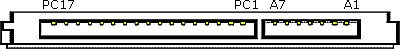
| PC1 | CDI | CARD detect input on the card |
| PC2 | GND | Device GND |
| PC3 | TBD | To Be Discussed (reserved) |
| PC4 | TBD | To Be Discussed (reserved) |
| PC5 | TBD | To Be Discussed (reserved) |
| PC6 | TBD | To Be Discussed (reserved) |
| PC7 | GND | Device GND |
| PC8 | LED1 | LED output on card |
| PC9 | LED2 | No Connect |
| PC10 | IO1 | Reserved IO (Write Protect, if enabled) |
| PC11 | IO2 | Reserved IO |
| PC12 | IO3 | Reserved IO |
| PC13 | PWR | +3.3V |
| PC14 | PWR | +3.3V |
| PC15 | PGND | Power GND |
| PC16 | PGND | Power GND |
| PC17 | CDO | Card detect CMOS output from the card |
 правильная
 с ошибками